
INSTRUCTION MANUAL Download
- Aviation
- Mobile
- Mobile
| Model | IC-A110 |
|---|---|
| Document | INSTRUCTION MANUAL |
| Note | |
| File size | 1.46MB |
About this Download Service.
Icom Inc. would like to advise User’s of the following regarding this download service for User Manuals and Service Manuals. If you agree to the following, push the AGREE button below to proceed.
The following apply to this download service.
- The ownership, copyright and other rights pertaining to all User Manuals and all of the contents of this site are the sole property of Icom Inc. Individual use of the Manuals is permitted, but the following are strictly prohibited.
- Reproduction, lease, alteration, public distribution or the creation of means to publicly distribute the Manuals.
- The transfer of the Manuals either for compensation or no compensation to a third party.
- The use of the Manuals either for profit or non-profit commercial use.
- The transfer of any and all photos, illustrations, data etc. in the Manuals.
- Do not alter in any way the Manuals or any of the contents of this site. Icom Inc. accepts no responsibility for faults and/or damages/losses caused as a result of alterations made by User’s.
- The content of the Manuals on this site, including legal content, specifications, addresses and phone numbers were correct at the time of publication and sale of the product. However, changes may have been made to update any change in such content.
- Icom Inc. reserves the right to change the content of the Manuals any time, and it is possible that in some cases the content of the Manuals on this site may differ slightly to that of the Manuals included in the product package at the time of purchase.
- The addition of notices, corrections and quick manuals to the product packaging is sometimes made. In some case, such additions to the content of the Manuals may not appear on this site.
- Reproduction of the content of the Manuals is permitted only when such reproduction is for the individual use by the person downloading the Manuals, and in accordance with the conditions of this download service.
- Icom Inc. accepts no responsibility, and is indemnified from any damages or losses caused as a result of the User using or not being able to use this download service.
- Icom Inc. reserves the right to stop, cancel or make changes to this download service without notice or obligation.
View the manual for the ICOM IC-A110 here, for free. This user manual comes under the category receivers and has been rated by 5 people with an average of a 7.8. This manual is available in the following languages: English. Do you have a question about the ICOM IC-A110?
Ask your question here
Frequently asked questions
Can’t find the answer to your question in the manual? You may find the answer to your question in the FAQs about the ICOM IC-A110 below.
Can bluetooth devices of different brands be connected to each other?
Yes, bluetooth is a universal method that allows different devices equipped with bluetooth to connect to each other.
What is bluetooth?
Bluetooth is a way of exchanging data wirelessly between electronic devices via radio waves. The distance between the two devices that exchange data can in most cases be no more than ten metres.
What is HDMI?
HDMI stands for High-Definition Multimedia Interface. An HDMI cable is used to transport audio and video signals between devices.
When is my volume too loud?
A volume above 80 decibels can be harmful to hearing. When the volume exceeds 120 decibels, direct damage can even occur. The chance of hearing damage depends on the listening frequency and duration.
How can I best clean my receiver?
A slightly damp cleaning cloth or soft, dust-free cloth works best to remove fingerprints. Dust in hard-to-reach places is best removed with compressed air.
Wat is Dolby Atmos?
Dolby Atmos is a technology that ensures that the sound is reflected from the ceiling to where you are listening. This makes it possible to create a 5.1 effect with only 1 speaker.
Is the manual of the ICOM IC-A110 available in English?
Yes, the manual of the ICOM IC-A110 is available in English .
Is your question not listed? Ask your question here
Document Download |
‹
›
Icom IC-A110 Manual Online:
3.5,
2712
votes
Icom IC-A110 User Manual
Icom IC-A110 User Guide
Icom IC-A110 Online Manual
Text of Icom IC-A110 User Guide:
More Instructions:
|
Icom IC-A110 Instruction manual
|
DOWNLOAD | |
|
Icom IC-A110 Service manual addendum
|
DOWNLOAD | |
|
Icom IC-A110 Service manual
|
DOWNLOAD | |
|
Icom IC-A110 Instruction manual
|
DOWNLOAD |
Related Products and Documents (Transceiver):
-
Icom IC-A22 Transceiver Instruction manual
IC-A22
icom/ic-a22.pdf, 63 -
Icom IC-703 Plus Transceiver Operation & user’s manual
IC-703 Plus
icom/ic-703-plus.pdf, 1 -
Icom IC-M88 Transceiver Instruction manual
IC-M88
icom/ic-m88.pdf, 40 -
Icom IC-H16T MKII Transceiver Instruction manual
IC-H16T MKII
icom/ic-h16t-mkii.pdf, 20 -
Icom ID-51E Transceiver Operation & user’s manual
ID-51E
icom/id-51e.pdf, 60 -
Icom IC-M90E Transceiver Instruction manual
IC-M90E
icom/ic-m90e.pdf, 40 -
Icom iC-FR5000 Transceiver Insrtuction manual
iC-FR5000
icom/ic-fr5000.pdf, 16 -
Icom IC-F1020 Transceiver Instruction manual
IC-F1020
icom/ic-f1020.pdf, 20
Comparable Devices:
| # | Manufacturer | Model | Document Type | File | Updated | Pages | Size |
|---|---|---|---|---|---|---|---|
| 1 | Garmin | Mobile 20 | Declaration of conformity | garmin/mobile-20-AYD.pdf | 06 Sep 2023 | 1 | 0.02 Mb |
| 2 | Epson | Stylus®Pro 4000 | Brochure & specs | epson/stylus-r-pro-4000-2ZU.pdf | 01 May 2025 | 6 | |
| 3 | SignaMax | 065-7434 | Configuration manual | signamax/065-7434-ZPX.pdf | 03 Aug 2024 | 669 | |
| 4 | NEC | LCD2010 — MultiSync — 20.1″ LCD Monitor | Specifications | nec/lcd2010-multisync-20-1-lcd-monitor-P8S.pdf | 11 Nov 2023 | 1 | |
| 5 | Panasonic | MA3SE02 | Specification sheet | panasonic/ma3se02-F28.pdf | 25 Feb 2025 | 3 | 0.19 Mb |
| 6 | GreenWorks | 24072 | Owner’s manual | greenworks/24072-RFI.pdf | 01 Mar 2025 | 24 |
Similar Resources:
Transceiver Instructions:
-
Sagem Cell Phone MY800X
Sagem MY800X User Manual (Operation & user’s manual), @L9H99I
MY800X, 64
-
PICO Controller C1310
Controller Operation & user’s manual (PICO C1310)
C1310, 5
-
Maytag Washer MHWC7500YW
#X18XZ9: MHWC7500YW Washer Energy manual
MHWC7500YW, 2
-
Yamaha Other T-09
#C87KDP: T-09 Other Owner’s manual
T-09, 14
-
GW Instek Measuring Instruments GPT-10000 Series
GPT-10000 Series (Measuring Instruments ePDF Guide, #2894O4)
GPT-10000 Series, 24
-
GRE Radio PSR-282
PSR-282 (Radio ePDF User Manual, #BUN982)
PSR-282, 14
-
Teka Cooktop EF/60 4G AI
#4X7N69 EF/60 4G AI: Teka Cooktop Owner Documentation
EF/60 4G AI, 16
-
Vertical Telephone Xcelerator IP IP2007
Manual for Vertical Xcelerator IP IP2007 Telephone
Xcelerator IP IP2007, 7
-
GoMax Electronics Switch SW-5004R
Switch #651828
SW-5004R, 8
-
PWS Water Filtration Systems BEV-340
Water Filtration Systems Getting started (PWS BEV-340)
BEV-340, 22
-
Electrolux Hob EHL8740FOK
Electrolux Hob EHL8740FOK Operation & user’s manual
EHL8740FOK, 20
-
Escient Media Player MP-200
PDF Guide (@XUU37Z), Escient MP-200 Media Player (Thu 10.2024)
MP-200, 263
Comments, Questions and Opinions:

SERVICE
MANUAL
VHF AIR BAND TRANSCEIVER
iA110
ORDERING PARTS
Be sure to include the following four points when ordering
replacement parts:
1. 10-digit order numbers
2. Component part number and name
3. Equipment model name and unit name
4. Quantity required
<SAMPLE ORDER>
1130008830 S.IC TB31207AFN IC-A110 MAIN UNIT 5 pieces
8810009130 Screw BT M3x12 NI-ZU IC-A110 Bottom cover 10 pieces
Addresses are provided on the inside back cover for your
convenience.
INTRODUCTION
This service manual describes the latest service information for the IC-A110 VHF AIR BAND TRANSCEIVER at the
time of publication.
MODEL
IC-A110
VERSION SYMBOL
General GEN
General-1 GEN-1
U.S.A. USA
U.S.A.-1 USA-1
To upgrade quality, any electrical or mechanical parts and
internal circuits are subject to change without notice or
obligation.
DANGER
NEVER connect the transceiver to an AC outlet or to a DC
power supply that uses more than 16 V. This will ruin the
transceiver.
DO NOT expose the transceiver to rain, snow or any liquids.
DO NOT reverse the polarities of the power supply when
connecting the transceiver.
DO NOT apply an RF signal of more than 20 dBm (100 mW)
to the antenna connector. This could damage the transceiver’s front end.
REPAIR NOTES
1. Make sure a problem is internal before disassembling
the transceiver.
2. DO NOT open the transceiver until the transceiver is
disconnected from its power source.
3. DO NOT force any of the variable components. Turn
them slowly and smoothly.
4. DO NOT short any circuits or electronic parts. An insu-
lated tuning tool MUST be used for all adjustments.
5. DO NOT keep power ON for a long time when the trans-
ceiver is defective.
6. DO NOT transmit power into a signal generator or a
sweep generator.
7. ALWAYS connect a 50 dB to 60 dB attenuator between
the transceiver and a deviation meter or spectrum analyzer when using such test equipment.
8. READ the instructions of test equipment thoroughly
before connecting equipment to the transceiver.

TABLE OF CONTENTS
SECTION 1 SPECIFICATIONS
SECTION 2 INSIDE VIEWS
SECTION 3 CIRCUIT DESCRIPTION
3 — 1 RECEIVER CIRCUITS…………………………………………………………………………………………………………….. 3 — 1
3 — 2 TRANSMITTER CIRCUITS ……………………………………………………………………………………………………… 3 — 3
3 — 3 PLL CIRCUITS………………………………………………………………………………………………… …………………….. 3 — 4
3 — 4 POWER SUPPLY CIRCUITS …………………………………………………………………………………………………… 3 — 5
3 — 5 PORT ALLOCATIONS …………………………………………………………………………………………………………….. 3 — 5
SECTION 4 ADJUSTMENT PROCEDURES
4 — 1 PREPARATION ……………………………………………………………………………………………………………………… 4 — 1
4 — 2 PLL ADJUSTMENT…………………………………………………………………………………………………………………. 4 — 3
4 — 3 TRANSMITTER ADJUSTMENT……………………………………………………………………………………………….. 4 — 3
4 — 4 RECEIVER ADJUSTMENT………………………………………………………………………………………………………. 4 — 5
SECTION 5 PARTS LIST
SECTION 6 MECHANICAL PARTS AND DISSASEMBLY
SECTION 7 SEMI-CONDUCTOR INFORMATION
SECTION 8 BOARD LAYOUTS
8 — 1 FRONT UNIT ………………………………………………………………………………………………….. …………………….. 8 — 1
8 — 2 MAIN UNIT…………………………………………………………………………………………………………………………….. 8 — 3
SECTION 9 BLOCK DIAGRAM
SECTION 10 VOLTAGE DIAGRAM
10 — 1 FRONT UNIT …………………………………………………………………………………………………………………………10 — 1
10 — 2 MAIN UNIT…………………………………………………………………………………………………………………………….10 — 2

1 — 1
SECTION 1 SPECIFICATIONS
‘‘
GENERAL
• Frequency coverage : 118.000–136.975 MHz
• Channel spacing : 25 kHz [GEN], [GEN-1]
25 kHz/8.33 kHz [USA], [USA-1]
• Type of emission : AM (6K00A3E)
• Number of memory channels : 20 channels
• Antenna connector : SO-239 (50 Ω)
• Power supply requirement : 13.75 V DC or 27.5 V DC (negative ground)
• Current drain (at 13.75 V DC) : Transmit 5.0 A
Receive max. audio output 4.0 A
stand-by 500 mA
• Frequency stability : ±5 ppm
• Usable temperature range : –30˚C to +60˚C; –22˚F to +140˚F
• Dimensions (projections not included) : 150(W) × 50(H) × 180(D) mm; 5
29
⁄32(W) × 131⁄32(H) × 73⁄32(D) in
• Weight (with ant., BP-209) : 1.5 g; 3 lb 5 oz
‘‘
TRANSMITTER
• RF output power (at 13.75 V DC) : 9.0 W (typical)
• Modulation system : Last stage modulation
• Input impedance : 600 Ω
• Modulation limitting : 70–100 %
• Audio harmonic distortion : Less than 10 % (at 85 % modulation)
• Ham and noise ratio : More than 40 dB
• Spurious emissions : –16 dBm or less (except ±62.5 kHz of operating frequency)
• Antenna requirements : Standard 50 Ω antenna with a VSWR < 3 : 1
‘‘
RECEIVER
• Receive system : Double conversion superheterodyne system
• Intermediate frequencies : 1st 38.85 MHz
2nd 450 kHz
• Sensitivity : Less than 1 µV at 6 dB S/N
• Squelch sensitivity : Less than 0.35 µV at threshold
• Selectivity :
• Spurious response rejection ratio : More than 74 dBµ
• Hum and noise : More than 25 dB
• Audio output power (at 13.75 V DC) : Ext SP More than 10.0 W at 10 % distortion with an 8 Ω load
Side tone More than 100 mW at 10 % distortion with an 500 Ω load
• Audio output impedance : Ext SP 8 Ω
Side tone 500 Ω
Specifications are measured in accordance with FCC Part87 and RTCA DO-186a.
(RTCA DO-186a: Class C/E, Class 4/6)
All stated specifications are subject to change without notice or obligation.
At 25 kHz channel spacing
At 8.33 kHz channel spacing
±8 kHz
±17 kHz
±25 kHz
Less than 6 dB
Less than 40 dB
Less than 60 dB
±2.778 kHz
±7.37 kHz
Less than 6 dB
Less than 60 dB
Low-pass filter
Antenna switching circuit
Crystal band pass filter
(FI1: FL-306)
Ceramic band pass filter
(FI3: CFWM450D)
Ceramic band pass filter
(FI4: CFG450H [USA/-1] only)
VCO circuit
APC amplifier
(Q11: 2SC4081)
Crystal band pass filter
(FI2: FL-307 [USA/-1] only)
Power complifier
(Q51: MRF137)
TCXO
(X1: CR-653)
2 — 1
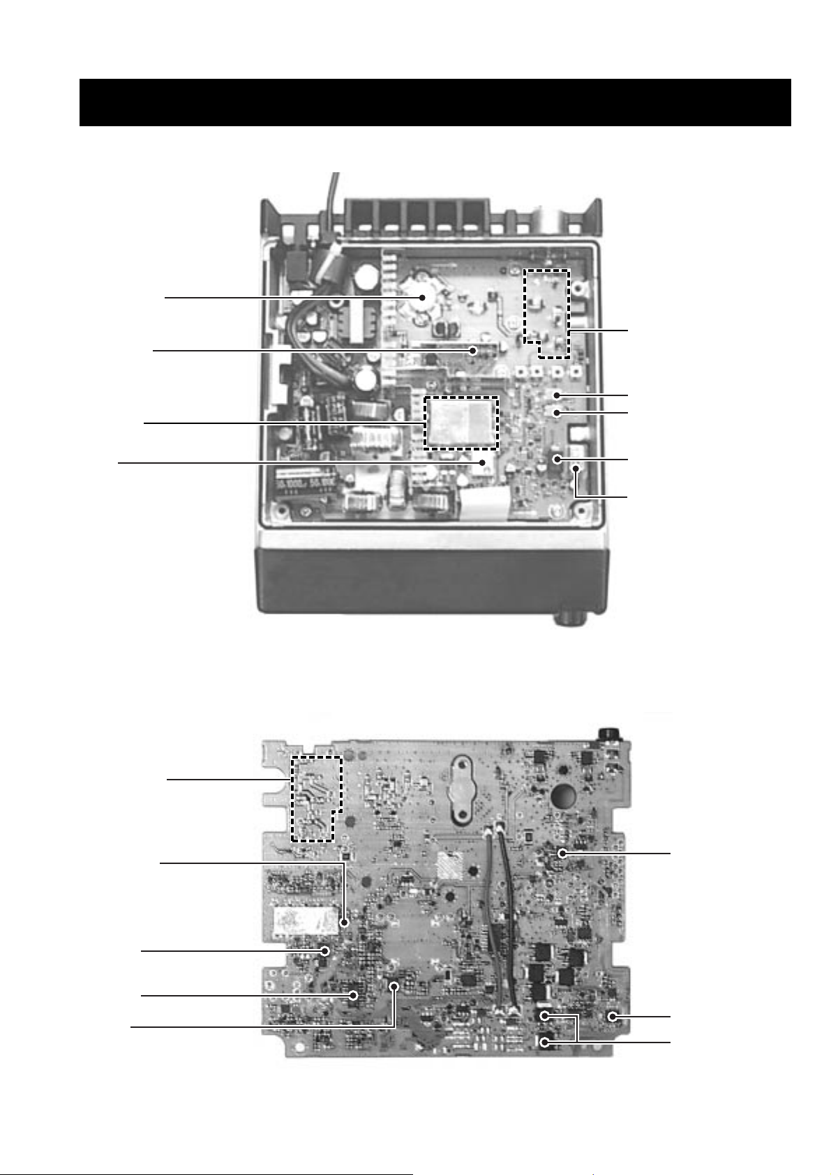
SECTION 2 INSIDE VIEWS
¡MAIN UNIT
<TOP VIEW>
AF amplifier
(IC37: TDA7233D)
RX 1st mixer
(Q2: 3SK184)
2nd IF IC
(IC40: TA31136FN)
PLL IC
(IC2: TB31207AFN)
PWM modulator
(IC44: µPC311)
EEPROM
(IC4: BA3308F)
Low-pass filter
Antenna switching circuit
AF power amplifier
(Q92,93: 2SK2414)

3 — 1
SECTION 3 CIRCUIT DESCRIPTION
3-1 RECEIVER CIRCUITS
3-1-1 ANTENNA SWITCHING CIRCUIT
The antenna switching circuit functions as a low-pass filter
while receiving. However, its impedance becomes very high
while D1 and D2 are turned ON. Thus transmit signals are
blocked from entering the receiver circuits. The antenna
switching circuit employs a λ⁄4 type diode switching system.
The passed signals are then applied to the RF amplifier circuit.
Received signals are passed through the low-pass filter (L2,
L3, L48, C1–C6, C330, C331). The filtered signals are
applied to the λ⁄4 type antenna switching circuit (D1, D2).
3-1-2 RF CIRCUIT
The RF circuit amplifies signals within the range of frequency coverage and filters out-of-band signals.
The signals from the antenna switching circuit are amplified
at the RF amplifier (Q1) after passing through the RX attenuator (D38, L52, R295), bandpass filter (L27, L8, C10,
C164, C165, C21) and two-stage tunable bandpass filters
(the first filter is consisted of D6, L9, C342, C405 and the
second filter is consisted of D37, L49, C23, C406). The
amplified signals are applied to the 1st mixer circuit (Q2,
gate 1) after out-of-band signals are suppressed at the
another two-stage tunable bandpass filters (D7, L10, C28,
C407 and D8, L11, C61, C553).
The tunable bandpass filters (D6–D8, D37) which employ
varactor diodes, track the filters and are controlled by the
PLL IC (IC2) via the tune buffer amplifier (Q79) using
“TUNE” signal. These diodes tune the center frequency of
an RF passband for wide bandwidth receiving and good
image response rejection.
3-1-3 1ST MIXER AND 1ST IF CIRCUITS
The 1st mixer circuit converts the received signal into a fixed
frequency of the 1st IF signal with a PLL output frequency.
By changing the PLL frequency, only the desired frequency
will pass through a crystal filter at the next stage of the 1st
mixer.
The filtered signals from the RF circuit are mixed at the 1st
mixer (Q2) with a 1st LO signal coming from the VCO circuit
to produce a 38.85 MHz 1st IF signal.
The 1st IF signal is applied to a pair of crystal filter [Wide
mode: FI1, Narrow mode: FI2] to suppress out-of-band signals. The filtered 1st IF signal is applied to the IF amplifier
(Q3), then applied to the 2nd mixer circuit (IC40, pin 16).
3-1-4 2ND MIXER AND 2ND IF CIRCUITS
The 2nd mixer circuit converts the 1st IF signal into a 2nd IF
signal. Adouble conversion superheterodyne system (which
converts receive signals twice) improves the image rejection
ratio and obtains stable receiver gain.
The 1st IF signal from the IF amplifier is applied to the 2nd
mixer section of the IF IC (IC2, pin 16), and is mixed with the
38.4 MHz 2nd LO signal to be converted into a 450 kHz 2nd
IF signal.
A2nd LO signal (38.4 MHz) is produced at the PLLcircuit by
tripling it’s reference frequency (12.8 MHz).
The 2nd IF signal from the 2nd mixer (IC2, pin 3) passes
through a ceramic filter [Wide mode: FL3, Narrow mode:
FI4] to remove unwanted heterodyned frequencies. It is then
amplified at the 2nd IF amplifiers (Q4–Q6).
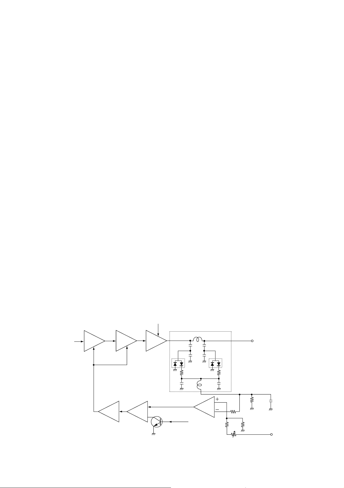
• Receiver construction
118.000–136.975 MHz
D1–D3 Q1
LPF
Ant SW
to AF circuit
D38
ATT
BPF
D6,
D37
Tuned Tuned XTAL
BPF
AM
DET
RF
AMP
«TUNE» signal
IF
AMP
Q6
Q4,
Q5
BPF
AMP
D7,
D8
IF
1st mixer
Q2
1st LO signal
79.15–98.125 MHz
from VCO circuit
Tripler
Q83, Q84
450 kHz
XTAL
BPF
FI3 [Wide],
FI4 [Narrow]
FI1 [Wide],
FI2 [Narrow]
38.85 MHz
BPF
12.8 MHz signal
from TCXO (X1)
3
2nd LO signal
38.4 MHz
2nd IF
IC
Q3
IF
AMP

3 — 2
3-1-5 AM DETECTOR CIRCUIT (MAIN UNIT)
The AM detector circuit converts the 2nd IF signal into AF
signals.
The amplified 2nd IF signal from the 2nd IF amplifier (Q6) is
applied to the AM detector circuit (Q7). It is then detected for
conversioin to AF signals.
The AF signals are applied to the AF circuit.
3-1-6 AF CIRCUIT (MAIN UNIT)
The AF circuit amplifies the demodulated AF signals to drive
a speaker.
The AF signals are passed through the low pass filter (IC31,
pin 1), and then applied to the MOD/AF select swtich (IC22,
pin 7).
The AF signals are amplified at the AF amplifier (IC42, pin
3), and are then passed through the RMUTE swtich (IC6)
and electric-volume switch (IC13, pins 14, 15) to control AF
level. The level controlled signals are then applied to the
mute switch (IC30, pin 1).
While in using the internal speaker or connecting outer
speaker jack, the AF signals are applied to the MOD/AF
swtich (IC48, pin 7) via the AF mute swtich (IC28). The
applied AF signals are compared at the PWM IC (IC44) with
the reference signal from the triangular wave oscillator
(IC45), and are then converted to the PWM wave form. The
AF signals are amplified at the FET driver (IC47) and AF
power amplifiers (Q92, Q93). The amplified AF signals are
applied to the SP mute switch (D66, Q101, Q100) via the
line filter (L62–L64, L81, C456, C457, C462, C463). The filtered AF signals are applied to the internal speaker via the
[EXT SP] jack (J7).
While in connecting the head set, the AF signals are amplified at the AF power amplifier (IC37, pin 8), and then applied
to the ACC connector (J6, pin 6) via the impedance convertor (T1).
3-1-7 SQUELCH CIRCUIT
(MAIN AND FRONT UNITS)
The squelch circuit cuts out AF signals when receiving no
modulated signal. When no voice modulation is included in
the signal, the squelch circuit cuts out the AF signal by comparing voice audio and noise audio components in the AF
detected signals.
The 2nd IF signal from the IF IC (MAIN unit; IC40, pin 3)
passes through the 450 kHz ceramic filter (Wide mode: FI3,
Narrow mode: FI4) to remove out-of-band signals, and then
applied to the IF amplifier.
A portion of the amplified 2nd IF signal from the IF amplifier
(MAIN unit; Q4) is applied to the IF amplifier section on the
IF IC (MAIN unit; IC40, pin 5). The amplified signal passes
through the RSSI section, and are then applied to the
squelch amplifier (MAIN unit; IC11, pin 1) as “RSSI” signal.
The amplified “RSSI” signal at IC11 is output from pin 4 as
“SQLI” signal, and is then applied to the CPU (FRONT unit;
IC1, pin 74). The CPU analyzes the noise condition and outputs the “AFMUT” signal via the output expander IC
(FRONT unit; IC5) to switch the SP mute switch (Q100,
Q101), etc. When connecting the head set, “RMUTE” signal
from the CPU via the output expander IC (FRONT unit; IC5)
is applied to the RMUTE circuit (MAIN unit; IC6, Q80, Q81).
Even when the squelch is closed, the mute switch (IC30)
opens at the moment of emitting beep tones.
3-1-8 AGC CIRCUIT (MAIN UNIT)
The AGC (Automatic Gain Control) circuit reduces signal
fading and keeps the audio output level constant.
AF signal from the AM detector circuit (Q7) is amplified at
AGC amplifiers (Q77, Q78). The amplified signal from Q77
is applied to the IF amplifier (Q4, Q5). The other amplified
signal from Q78 is applied to the RF amplifier (Q1), and the
RX attenuator (D38) via the buffer amplifier (Q73).
These amplifiers reduce the amplifier gain of IF amplifiers
(Q4, Q5) and the RF amplifier (Q1) while receiving a strong
signal.
• AGC circuit
From the ant.
D38
RX ATT
Q73
Buffer
RF
AMP
Q1
1st mixer
Q2
XTAL
BPF
IF
AMP
Q3
2nd mixer
IC40
«IF AGC» signal
«RF AGC» signal
BPF
Q4, Q5
IF
AMP
Q6
IF
AMP
to AF circuit
D7
AM
DETECTOR
Q77
AGC
AMP
Q78
AGC
AMP
3 — 3
3-2 TRANSMITTER CIRCUITS
3-2-1 MICROPHONE AMPLIFIER CIRCUIT
(MAIN UNIT)
The microphone amplifier circuit amplifies audio signals
from the microphone, within +6 dB/octave pre-emphasis
characteristics (300 Hz–3 kHz), to a level needed for the
modulation circuit.
The AF signals from the microphone are applied to the
IN/EXT MIC switch (IC16, pin 7) via the “MIC” signal. When
using a headset, “EXTMIC” signal are applied to the external switch (IC16, pin 6) via R336 to adjust the external
microphone level. The output signal from IC16 (pin 1) are
applied to the ALC amplifier (IC4, pin 9) via R110 to adjust
the microphone sensitivity.
The output signal from IC4 (pin 7) are amplified at the AF
amplifier (IC5), and then applied to the MOD/AF switch via
the high-pass filter (IC51) and low-pass filter (IC19) to filter
out RF components. The filtered signals are applied to the
modulation circuit.
3-2-2 MODULATION CIRCUIT (MAIN UNIT)
The modulation circuit modulates the VCO oscillating signal
(RF signal) using the microphone AF signal.
The audio signals are passed through the MOD/AF switch
(IC48, pin 6) via the modulation depth adjustment pot R121.
The signals are converted to the PWM wave form at the
PWM (Pulse-Width-Modulation) IC (IC44, pin 3), and power
amplified at the FET driver (IC47, pin 5) and power MOS
FET (Q92, Q93). The power-amplified signals are passed
through the line filter (L62–L64, L81, C456, C457, C462,
C463, C468), and then applied to the drain of power amplifier (Q51) for the last stage modulation.
3-2-3 DRIVE/POWER AMPLIFIER CIRCUITS
(MAIN UNIT)
The amplifier circuit amplifies the VCO oscillating signal to
the output power level.
The signal from the buffer amplifiers (Q14, Q15) is passed
through the TX/RX switch (D11), and is amplified at the preamplifier (Q42), pre-drivers (Q20, Q21) and the power
amplifier (Q51) to obtain 9 W of RF power.
The amplified signal is passed through the antenna swtiching circuit (D3) and low-pass filter, and is then applied to the
antenna connector.
3-2-4 APC CIRCUIT (MAIN UNIT)
The APC (Automatic Power Control) circuit protects the
drive and power amplifiers from mismatched output loads.
The APC detector circuit (D4, D5) detects forward and
refrected signals respectively. The combined voltage is at a
minimum level when the antenna is matched at 50 Ω and is
increased when it is mismatched.
The detected voltage is applied to one of the APC controller
inputs (IC50, pin 3) and a power setting voltage is applied to
the other input (pin 1). When the antenna impedance is mismatched, the detected voltage exceeds the reference voltage. Thus the bias voltage of the pre-drivers is decreased.
• APC control circuit
Pre-amplified signal
(from MAIN unit; Q42)
PRE
DRIVE
Q20
Q98
«MOD V» signal from the AF power amplifiers
(MAIN unit; Q92, Q93)
PWR
CNT
PRE
DRIVE
Q21
Q51
PWR
AMP
Q11
APC
AMP
Power detector circuit
C14 C13
C17
Q99
«TMUT» signal from the
expander IC
(Front unit; IC5; pin 14)
D5
C18
IC50
L6
C16
D4
R2R3
L75
C19
APC
CNT
(Power adjustment)
R148
R149
R150
to the Antenna
R153
R151
C139
T8
3 — 4
3-3 PLL CIRCUIT
3-3-1 GENERAL (MAIN UNIT)
A PLL circuit provides stable oscillation of the transmit frequency and receive 1st LO frequency. The PLL output compares the phase of the divided VCO frequency to the reference frequency. The PLL output frequency is controlled by
the divided ratio (N-data) of a programmable divider.
The PLL circuit contains of the TX-VCO and RX-VCO circuits. The oscillated signals are applied to the buffer amplifiers (Q43, Q12) then applied to the PLL IC (IC2, pin 8). IC2
is a dual PLL IC which controls VCO circuits for TX and RX.
The PLL circuit, using a one chip PLL IC (IC2), directly generates the transmit frequency and receive 1st IF frequency
with VCOs. The PLL sets the divided ratio based on serial
data from the CPU on the FRONT unit and compares the
phases of VCO signals with the reference oscillator frequency. The PLL IC detects the out-of-step phase and output from pin 9 for TX and RX, respectively. The reference
frequency (12.8 MHz) is oscillated at X1.
3-3-2 TX LOOP
The generated signal at the TX-VCO (Q44, D64) enters the
PLL IC (IC2, pin 8), and is divided at the programmable
divider section and is then applied to the phase detector
section.
The phase detector compares the input signal with a reference frequency, and then outputs the out-of-phase signal
(pulse-type signal) from pin 9.
The pulse-type signal is converted into DC voltage (lock
voltage) at the loop filter (R61, R62, C59, C60), and then
applied to the varactor diode (D64) of the TX-VCO to stabilize the oscillated frequency.
3-3-3 RX LOOP
The generated signal at the RX-VCO (Q59, D65) enters the
PLL IC (IC2, pin 8), and is divided at the programmable
divider section. The divided signal is then applied to the
phase detector section.
The phase detector compares the input signal with a reference frequency, and then outputs the out-of-phase signal
(pulse-type signal) from pin 9.
The pulse-type signal is converted into DC voltage (lock
voltage) at the loop filter (R61, R62, C59, C60), and then
applied to the varactor diode (D65) of the RX-VCO to stabilize the oscillated frequency. The lock voltage is also used
for the receiver circuit for the bandpass filter center frequency. The lock voltage from the PLL IC (IC2, pin 9) passes
through the low-pass filter, and is applied to the tune buffer
amplifier (Q79). The amplified signal is applied to the RF
bandpass filters (D7, D8 and D6, D37) via the tune adjustment pot (R59).
3-3-4 VCO CIRCUIT
The VCO outputs from Q44 (TX) and Q59 (RX) are buffer
amplified at Q43, and are applied to the buffer amplifiers
(Q14, Q15). The amplified signal is applied to the T/R switch
(D10, D11). The receive LO signal is applied to the 1st mixer
circuit (Q2), and the transmit signal is applied to the preamplifier (Q42).
A portion of the VCO signal is amplified at the buffer amplifier (Q12), and then fed back to the PLL IC (IC2, pin 8).
• PLL circuit
Shift register
Prescaler
Phase
detector
Loop
filter
Programmable
counter
Programmable
divider
TCXO (X1)
12.8 MHz
Q44,
D64
TX VCO
RX VCO
Buff.
D10
D11
Q12
Q43
3
4
5
SCK
IC2 (PLL IC)
SO
PLSTB
to transmitter circuit
to 1st mixer circuit (Q2)
14
9
LPF
8
Q59,
D65
Buff.
Q14
Buff.
Q15
TX/RX
switch
Buff.
3
Q83, Q84
to the RF BPF
(D7 and D8, D6 and D37)
38.4 MHz 2nd LO signal
to the 2nd IF IC (IC40, pin 2)
Tune
buff.
R59
(RF BPF adjustment)
Q79

3 — 5
3-4 POWER SUPPLY CIRCUITS
VOLTAGE LINES (MAIN UNIT)
LINE
VCC
8V
+5V
CPU5V
T8
R8
DESCRIPTION
The voltage from the external DC power connector which is controlled by the power switch
([VOL] control).
Common 8 V converted from the VCC line by the
+8 V regulator circuit (IC29). The output voltage
is applied to the +5 V regulator circuit (IC7), the
ripple filter (Q16), and etc.
Common 5 V converted from the 8V line by the
+5V regulator (IC7) and +5V current amplifier
(Q22, Q23, D15) circuits. The output voltage is
applied to the electric volume IC (IC13), buffer
amplifiers (Q68, Q69), and etc.
Common 5 V converted from the VCC line by +8
V regulator (Q82, D35) and +5 V regulator circuits (IC26). The output 5 V voltage is applied to
the CPU (FRONT unit; IC1).
8 V for transmitter circuits regulated by the +8 V
regulator circuit (IC29).
8 V for receiver circuits regulated by the +8 V
regulator circuit (IC29).
3-5 PORT ALLOCATIONS
3-5-1 OUTPUT EXPANDER IC (FRONT unit: IC5)
Pin
number
4, 5
6
7
11
12
13
14
Port
name
LED1,
LED2
TRC
R/T
SMUT
AFMUT
RMUT
TMUT
Description
Outputs backlight control signals.
Outputs control signal to the MOD/AF
swtich (MAIN unit: IC48, pin 5) and
etc.
High:While transmitting.
Outputs control signal to the TX/RX
switch (MAIN unit: Q58, pin 1) for
VCO.
Low: While transmitting.
Outputs AF mute swtich (MAIN unit:
IC30, Q86, Q75, Q74, D43) control
signal.
Low: While squelched.
Outputs control signal to the mute
switch (MAIN unit; Q100, Q101, D66)
for speaker amplifier, and etc.
Low: While the speaker output is
muted.
Outputs RMUTE switch (IC6) control
signal.
Low: While squelched.
Outputs T8 regulator control signal.
Low: When TX is muted.
LED1
Low
High
Low
High
LED2
Low
Low
High
High
Backlight condition
Light OFF
No establishment
Light ON, Dimmer ON
Light ON, Dimmer OFF

Description
Input ports for the key matrix.
Input port for the CPU reset signal.
Outputs control signal for the power
supply circuit.
High:Power is ON.
Outputs beep audio signals.
Outputs clock signal to the EEPROM
(FRONT unit; IC4, pin 6).
Outputs data signal to the EEPROM
(FRONT unit; IC4, pin 5).
Outputs chip select signal to the EEP-
ROM (FRONT unit; IC4, pin 1).
Input port for the [DIAL] control signal.
Outputs control signal to the expander
IC (FRONT unit; IC5, pin 15).
Outputs strobe signals to the
expander IC (FRONT unit; IC5, pin 1).
Outputs chip select signal to the elec-
tric volume (MAIN unit; IC13).
Low: While volume is controlled.
Outputs serial clock to the PLL IC
(MAIN unit; IC2, pin 3), the expander
IC (FRONT unit; IC5, pin 3) and the
electric volume (MAIN unit; IC13, pin
8).
Input port for the data signal from the
EEPROM (FRONT unit; IC4, pin 2).
Outputs serial data to the PLL IC
(MAIN unit; IC2, pin 4), the expander
IC (FRONT unit; IC5, pin 2) and the
electric volume (MAIN unit; IC13, pin
9).
Outputs strobe signals to the PLL IC
(MAIN unit; IC2, pin 5).
Outputs 2nd IF filter’s select signal.
High:While wide is selected.
Input port for the unlock signal from
the PLL IC (MAIN unit; IC2, pin 11).
Low: PLL is unlocked.
Input port for the cloning signal.
Output port for the cloning signal.
Input port for the POWER switch.
Low: While POWER switch is
pushed
Input port for the squelch signal.
Port
name
KR4
RESET
PSWC
BEEP
ECK
ESO
ECS
DLA,
DLB
OE
EXSTB
VCS
SCK
ESI
SO
PLSTB
FISW
UNLK
CLIN
CLO
PSW
SQLI
Pin
number
1, 2, 3,
5, 8, 12
9
10
11
13
14
15
16,
17
18
19
20
21
22
23
24
25
69
70
71
72
74
3 — 6
Pin
number
76
77
78–80
Port
name
HANG
PTT
KR1–KR2
Description
Input port for the microphone hanger
detection signal.
Low: Microphone on hook.
Input port for the PTT switch.
High:While PTT switch is pushed.
Input ports for the key matrix.
3-5-2 CPU (FRONT unit; IC1)
4-1 PREPARATION
• Some versions may need the optional CS-A110 CLONING SOFTWARE and OPC-478, OPC-592
CLONING CABLE for setting the
adjustment frequency.
• All adjustments must be performed on the [Wide] mode.
■ REQUIRED TEST EQUIPMENT
4 — 1
SECTION 4 ADJUSTMENT PROCEDURES
■ VFO CHANNEL ID LIST
• Channel spacing: 8.33/25 kHz [USA/USA-1] • Channel spacing: 25 kHz [GEN/GEN-1]
EQUIPMENT
DC power supply
RF power meter
(terminated type)
Frequency counter
Modulation analyzer
Distortion meter
External speaker
GRADE AND RANGE
Output voltage : 13.75 V DC
Current capacity : 10 A or more
Measuring range : 1–50 W
Frequency range : 50–300 MHz
Impedance : 50 Ω
SWR : Less than 1.2 : 1
Frequency range : 0.1–300 MHz
Frequency accuracy: ±1 ppm or better
Sensitivity : 100 mV or better
Frequency range : DC–300 MHz
Measuring range : 0 to 100 %
Frequency range : 1 kHz±10 %
Measuring range : 1 to 100 %
Impedance : 8 Ω
EQUIPMENT
DC voltmeter
Digital multimeter
Audio generator
Standard signal
generator (SSG)
AC millivoltmeter
Attenuator
Terminator
GRADE AND RANGE
Input impedance : 50 kΩ/V DC or better
Input impedance : 10 MΩ/V DC or better
Frequency range : 300–3000 Hz
Measuring range : 1–500 mV
Frequency range : 0.1–300 MHz
Output level : 0.1 µV–32 mV
(–127 to –17 dBm)
Measuring range : 10 mV–10 V
Power attenuation : 40 or 50 dB
Capacity : 50 W or more
Impedance : 50 Ω
Capacity : 50 W or more
Operating Freq.
(MHz)
118.0000
118.0000
118.0083
118.0167
118.0250
118.0250
118.0333
118.0417
118.0500
118.0500
118.0583
118.0667
118.0750
118.0750
118.0833
118.0917
118.1000
118.1000
etc
Channel spacing
(kHz)
25
8.33
8.33
8.33
25
8.33
8.33
8.33
25
8.33
8.33
8.33
25
8.33
8.33
8.33
25
8.33
Channel ID
(Displayed Freq.)
118.000
118.005
118.010
118.015
118.020
118.030
118.035
118.040
118.050
118.055
118.060
118.065
118.070
118.080
118.085
118.090
118.100
118.105
Operating Freq.
(MHz)
118.0000
118.0250
118.0500
118.0750
118.1000
etc
Channel spacing
(kHz)
25
25
25
25
25
Channel ID
(Displayed Freq.)
118.000
118.025
118.050
118.075
118.100
Loading…
Icom IC-A110 Instruction Manual
Icom IC-A110 Transceiver Specification
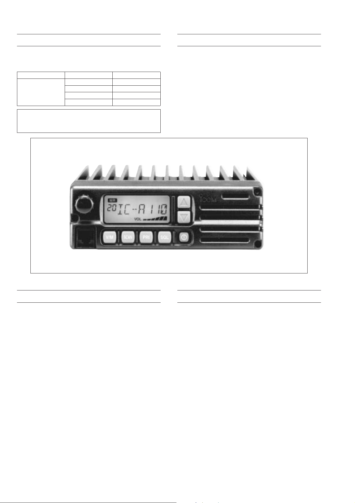
The Icom IC-A110 Transceiver is a high-performance VHF air band radio designed for ground-based communications in aviation environments. It operates in the VHF frequency range of 118.000 to 136.975 MHz, ensuring comprehensive coverage of the civil aviation band. The transceiver supports simplex communication, facilitating clear and reliable transmission and reception of voice signals. With a robust RF output power of 36 watts, it provides strong signal strength, essential for maintaining communication over extended distances.
The IC-A110 features a large, backlit LCD display that enhances visibility in various lighting conditions, allowing for easy reading of frequency settings and operational status. The front panel is user-friendly, with well-organized controls that enable quick access to essential functions. The transceiver includes 20 memory channels, enabling users to store and quickly recall frequently used frequencies, streamlining operations in busy air traffic environments.
The device’s construction emphasizes durability, with a rugged, die-cast aluminum chassis that provides superior protection against mechanical shocks and environmental conditions. It complies with military standards for temperature, humidity, and vibration, ensuring reliable performance in harsh environments. Advanced audio processing features, such as noise reduction and automatic gain control, contribute to clear audio quality, even in noisy surroundings.
The IC-A110 supports both 12V and 24V DC power sources, offering flexibility for installation in various vehicles and ground stations. Additional features include a side tone function for effective audio monitoring and an external speaker jack for enhanced audio output. With its blend of robust performance, user-friendly design, and reliable construction, the Icom IC-A110 is a dependable choice for professional aviation communication needs.
Icom IC-A110 Transceiver F.A.Q.
To perform a factory reset on the Icom IC-A110, turn off the transceiver. While holding down the ‘CLR’ and ‘DIAL’ buttons, turn the power back on. Release the buttons after the display shows ‘CLr’. This will reset the transceiver to its factory default settings.
To program frequencies, press the ‘DIAL’ button to enter the frequency setting mode. Use the tuning knob to select the desired frequency. Press ‘ENT’ to save. Repeat the process for additional frequencies. Always ensure you are programming legal and appropriate frequencies for your region.
Check the antenna connection for any loose or damaged cables. Ensure the microphone is functioning correctly and not obstructed. Verify that the transceiver is set to the correct power output setting. If the problem persists, consult a professional technician.
Regularly inspect the antenna and cable connections. Clean the exterior surface with a soft, dry cloth. Avoid exposure to extreme temperatures and moisture. Periodically check that the firmware is up to date and test the audio clarity.
Adjust the squelch level by rotating the ‘SQL’ knob. Turn clockwise to increase the squelch level, reducing background noise, and counterclockwise to decrease it. Fine-tune until you achieve the desired balance between noise and signal reception.
Yes, the IC-A110 can be connected to an external speaker. Use the external speaker jack located on the back panel of the transceiver. Ensure the speaker impedance matches the transceiver’s requirements to avoid damage.
To update the firmware, connect the IC-A110 to a computer using the appropriate interface cable. Download the latest firmware from the Icom website. Follow the instructions provided with the firmware update tool to complete the installation.
To improve battery life, ensure the transceiver is turned off when not in use. Reduce the transmission power level if high power is not necessary. Avoid excessive use of backlighting and other power-consuming features when possible.
Check the power connection and ensure the power source is functioning. Inspect the fuse in the power cable for any damage and replace if necessary. If the transceiver still does not turn on, consult the user manual or seek professional assistance.
To set up memory channels, tune to the desired frequency and press ‘MR’ to enter memory mode. Select an empty channel using the tuning knob and press ‘ENT’ to store the frequency. Repeat for additional channels as needed.