
6-9-16, Kamihigashi, Hirano-ku, Osaka 547-0002, Japan
Phone : 06 6793 5302
Fax : 06 6793 0013
Communication Equipment
Himmelgeister Str. 100, D-40225 Düsseldorf, Germany
Phone: 0211 346047 Fax : 0211 333639
URL : http://www.icomeurope.com
Unit 9, Sea St., Herne Bay, Kent, CT6 8LD, U.K.
Phone: 01227 741741 Fax : 01227 741742
URL : http://www.icomuk.co.uk
Zac de la Plaine, Rue Brindejonc des Moulinais
BP 5804, 31505 Toulouse Cedex, France
Phone: 561 36 03 03 Fax : 561 36 03 00
URL : http://www.icom-france.com
Crta. de Gracia a Manresa Km. 14,750
08190 Sant Cugat del Valles Barcelona, SPAIN
Phone: (93) 590 26 70 Fax : (93) 589 04 46
URL : http://www.icomspain.com
<
Corporate Headquarters
>
2380 116th Avenue N.E., Bellevue, WA 98004, U.S.A.
Phone: (425) 454-8155 Fax : (425) 454-1509
URL : http://www.icomamerica.com
<
Customer Service
>
Phone: (425) 454-7619
A.C.N. 006 092 575
290-294 Albert Street, Brunswick, Victoria, 3056, Australia
Phone: 03 9387 0666 Fax : 03 9387 0022
URL : http://www.icom.net.au
6F No. 68, Sec. 1 Cheng-Teh Road, Taipei, Taiwan, R.O.C.
Phone: (02) 2559 1899 Fax : (02) 2559 1874
3071 #5 Road, Unit 9, Richmond, B.C., V6X 2T4, Canada
Phone: (604) 273-7400 Fax : (604) 273-1900
URL : http://www.icomcanada.com
INTRODUCTION
This service manual describes the latest service information
for the
IC-F4GT and IC-F4GS
at the time of publication.
NEVER connect the transceiver to an AC outlet or to a DC
power supply that uses more than 16 V. Such a connection
could cause a fire hazard and/or electric shock.
DO NOT expose the transceiver to rain, snow or any liquids.
DO NOT reverse the polarities of the power supply when con-
necting the transceiver.
DO NOT apply an RF signal of more than 20 dBm (100mW)
to the antenna connector. This could damage the transceiver’s front end.
Be sure to include the following four points when ordering
replacement parts:
1. 10-digit order numbers
2. Component part number and name
3. Equipment model name and unit name
4. Quantity required
<SAMPLE ORDER>
1130007610 S.IC µPD3140GS IC-F4GT MAIN UNIT 1 pieces
8810009510 Screw BT M2 x 4 NI-ZU IC-F4GS Chassis 10 pieces
Addresses are provided on the inside back cover for your
convenience.
1. Make sure a problem is internal before disassembling the transceiver.
2. DO NOT open the transceiver until the transceiver is disconnected from its power source.
3. DO NOT force any of the variable components. Turn them slowly and smoothly.
4. DO NOT short any circuits or electronic parts. An insulated turning tool MUST be used for all adjustments.
5. DO NOT keep power ON for a long time when the transceiver is defective.
6. DO NOT transmit power into a signal generator or a sweep generator.
7. ALWAYS connect a 40 dB to 50 dB attenuator between the transceiver and a deviation meter or spectrum analyzer when
using such test equipment.
8. READ the instructions of test equipment thoroughly before connecting equipment to the transceiver.
To upgrade quality, all electrical or mechanical parts and
internal circuits are subject to change without notice or obligation.
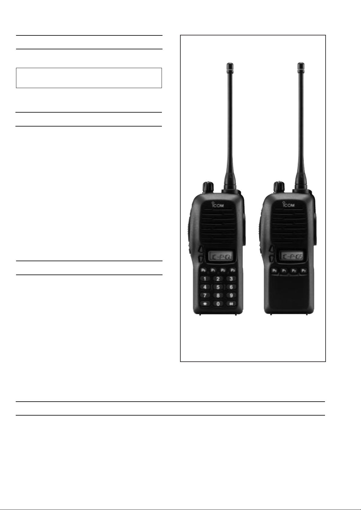
IC-F4GT IC-F4GS

TABLE OF CONTENTS
SECTION 1 SPECIFICATIONS
SECTION 2 INSIDE VIEWS
SECTION 3 DISASSEMBLY AND OPTION INSTRUCTIONS
3-1 DISASSEMBLY INSTRUCTION . . . . . . . . . . . . . . . . . . . . . . . . . . . . . . . . . . . . . . . . . . . . . .3-1
3-2 OPTIONAL UNIT INSTALLATIONS . . . . . . . . . . . . . . . . . . . . . . . . . . . . . . . . . . . . . . . . . . . .3-2
SECTION 4 CIRCUIT DESCRIPTION
4-1 RECEIVER CIRCUITS . . . . . . . . . . . . . . . . . . . . . . . . . . . . . . . . . . . . . . . . . . . . . . . . . . . . .4-1
4-2 TRANSMITTER CIRCUITS . . . . . . . . . . . . . . . . . . . . . . . . . . . . . . . . . . . . . . . . . . . . . . . . .4-1
4-3 PLL CIRCUITS . . . . . . . . . . . . . . . . . . . . . . . . . . . . . . . . . . . . . . . . . . . . . . . . . . . . . . . . . . .4-2
4-4 POWER SUPPLY CIRCUITS . . . . . . . . . . . . . . . . . . . . . . . . . . . . . . . . . . . . . . . . . . . . . . . .4-3
4-5 CPU PORT ALLOCATIONS . . . . . . . . . . . . . . . . . . . . . . . . . . . . . . . . . . . . . . . . . . . . . . . . .4-4
SECTION 5 ADJUSTMENT PROCEDURES
5-1 PREPARATION . . . . . . . . . . . . . . . . . . . . . . . . . . . . . . . . . . . . . . . . . . . . . . . . . . . . . . . . . .5-1
5-2 PLL ADJUSTMENT . . . . . . . . . . . . . . . . . . . . . . . . . . . . . . . . . . . . . . . . . . . . . . . . . . . . . . .5-4
5-3 SOFTWARE ADJUSTMENT . . . . . . . . . . . . . . . . . . . . . . . . . . . . . . . . . . . . . . . . . . . . . . . . .5-5
SECTION 6 PARTS LIST
SECTION 7 MECHANICAL PARTS AND DISASSEMBLY
SECTION 8 SEMI-CONDUCTOR INFORMATION
SECTION 9 BOARD LAYOUTS
SECTION 10 BC-137 OPTIONAL DESKTOP CHARGER INFORMATION
10-1 PARTS LIST . . . . . . . . . . . . . . . . . . . . . . . . . . . . . . . . . . . . . . . . . . . . . . . . . . . . . . . . . . . . .10-1
10-2 DISASSEMBLY INFORMATION . . . . . . . . . . . . . . . . . . . . . . . . . . . . . . . . . . . . . . . . . . . . . .10-1
10-3 VOLTAGE DIAGRAM . . . . . . . . . . . . . . . . . . . . . . . . . . . . . . . . . . . . . . . . . . . . . . . . . . . . . .10-2
10-4 BOARD LAYOUT . . . . . . . . . . . . . . . . . . . . . . . . . . . . . . . . . . . . . . . . . . . . . . . . . . . . . . . . .10-2
SECTION 11 BLOCK DIAGRAM
SECTION 12 VOLTAGE DIAGRAM

1 — 1
SECTION 1 SPECIFICATIONS
‘‘
GENERAL
• Frequency coverage : 440.000–470.000 MHz
• Type of emission : 8K50F3E
• Number of channels : 32 ch (16 channels × 2 banks: 2-BANK version), 16 ch (16 channel version)
• Power supply requirement : 7.2 V DC (negative ground; supplied battery pack)
• Current drain (approx.) : Transmit at High (4.0 W) 1.55 A
at Low (1.0 W) 800 mA
Receive rated audio 250 mA
stand-by 70 mA
• Frequency stability : ±0.00025 %
• Usable temperature range : –30˚C to +60˚C; –22˚F to +140˚F
• Dimensions (projections not included) : 54(W) × 132(H) × 35(D) mm; 2
5
⁄32(W) × 5 3⁄16(H) × 1 3⁄8(D) in.
• Weight (with ant., BP-209) : 355 g; 12.5 oz.
‘‘
TRANSMITTER
• RF output power (at 7.2 V DC) : 4 W / 1 W (High / Low)
(with supplied battery pack)
• Modulation system : Variable reactance frequency modulation
• Maximum frequency deviation : ±2.5 kHz
• Spurious emissions : 73 dBc (typical)
• Adjacent channel power : 60 dB (typical)
• Transmitter audio distortion : Less than 3% at 1 kHz, 40% deviation
• Limitting charact of modulator : 70–100% of max. deviation
• Ext. microphone connector : 3-conductor 2.5(d) mm (
1
⁄10”)/2.2 kΩ
‘‘
RECEIVER
• Receive system : Double conversion superheterodyne system
• Intermediate frequencies : 1st 46.35 MHz
2nd 450 kHz
• Sensitivity : 0.3 µV at 12 dB SINAD (typical)
• Squelch sensitivity : 0.3 µV at threshold (typical)
• Adjacent channel selectivity : 65 dB (typical)
• Spurious response rejection : 70 dB (typical)
• Intermodulation rejection ratio : 70 dB (typical)
• Hum and noise : 40 dB (typical)
• Audio output power (at 7.2 V DC) : 500 mW typical at 5% distortion with an 8 Ω load
• Ext. speaker connector : 3-conductor 3.5(d) mm (
1
⁄8”)/8 Ω
Specifications are measured in accordance with EIA/TIA-603.
All stated specifications are subject to change without notice or obligation.
2 — 1
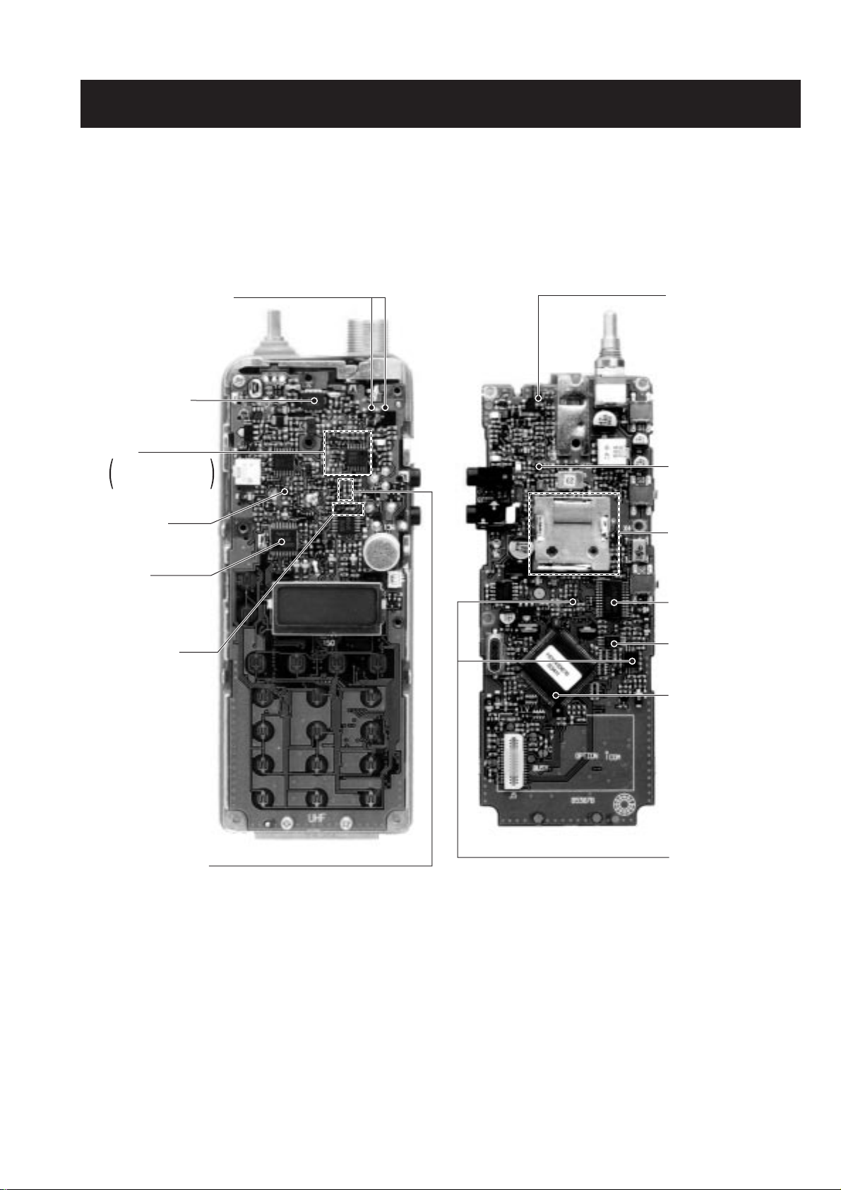
SECTION 2 INSIDE VIEWS
• MAIN UNIT
Antenna switcing circuit
(D1: 1SV307)
1st mixer
(Q13: 3SK239A)
VCO circuit
D/A converter
(IC10: M62363FP-650C)
EEPROM
(IC7: HN58X2432TI)
CPU
(IC8: HD6433876B34H)
Low pass filter circuit
Antenna switcing circuit
(D2, D8: MA77)
Power amplifier
(Q1: 2SK2974)
IF amplifier
(Q14: 2SC4215 O)
PLL IC
(IC1: µPD3140GS)
TX/RX switch
(D3, D4: MA77)
Mic amplifier circuit
APC
IC3A: NJM3403AV
Q37: DTA144EU
3 — 1
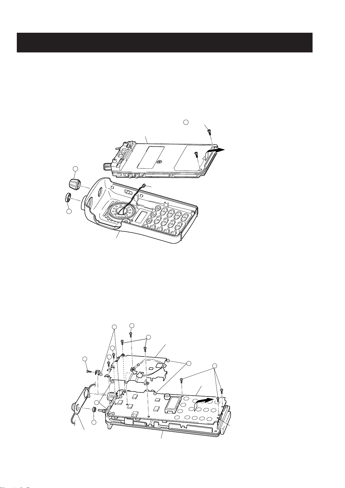
SECTION 3 DISASSEMBLY AND OPTION INSTRUCTIONS
3-1 DISASSEMBLY INSTRUCTION
• REMOVING THE CHASSIS PANEL
1 Unscrew 1 nut A, and remove 1 knob B.
2 Unscrew 2 screws C.
3 Take off the chassis in the direction of the arrow.
4 Unplug J6 to separate front panel and chassis.
• REMOVING THE MAIN UNIT
1 Remove the searing rubber.
2 Unsolder 3 points D, and unscrew 1 nut E.
3 Unscrew 3 screws F and 6 screws G (silver, 2 mm) to separate the chassis and the MAIN unit.
4 Take off the MAIN unit in the direction of the arrow.
(nickel, 2 mm) x 2
Front panel
Chassis
J6 (Speaker connector)
B
C
A
D
F
F
G
G
G
D
(silver, 2 mm) x 6
E
Shield cover
Guide holes
MAIN unit
Sealing rubber
Chassis
D
F
3 — 2
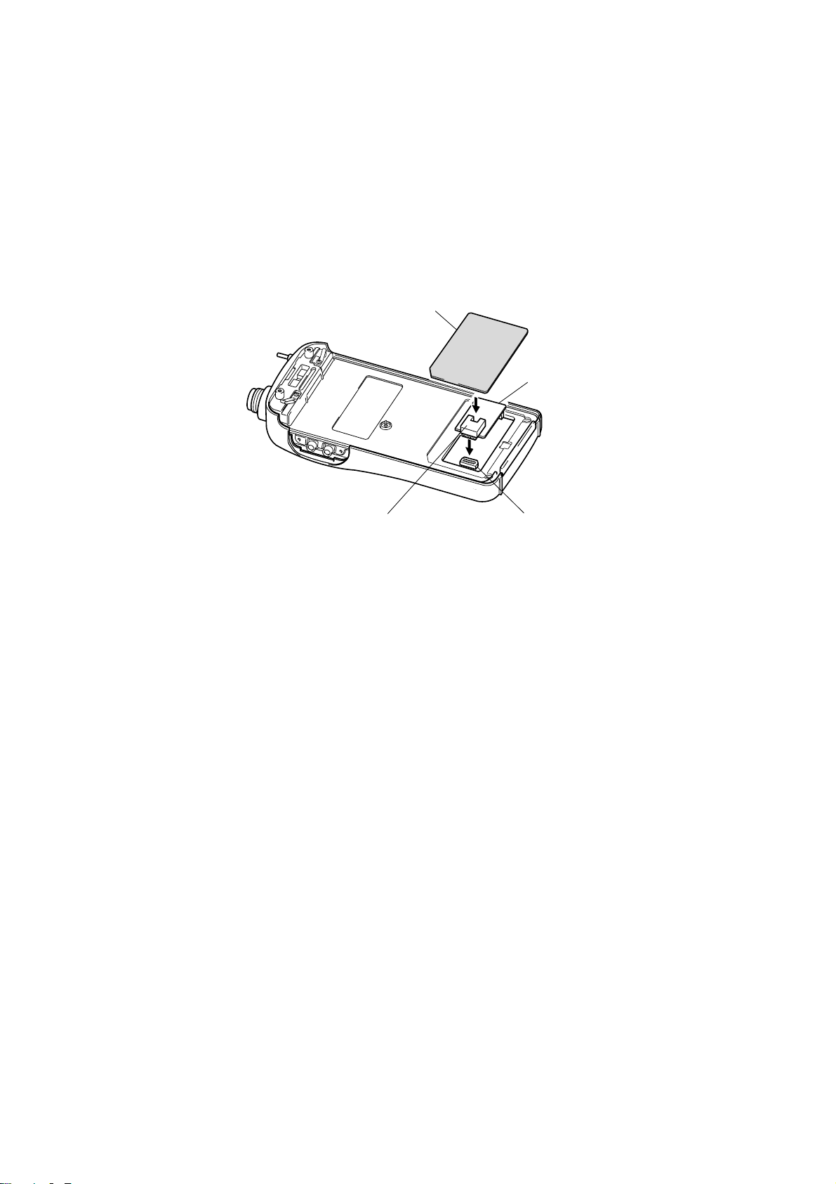
3-2 OPTIONAL UNIT INSTALLATIONS
1 Remove the option cover.
2 Remove the bottom protective paper of spoge.
3 Connect one of UT-96, UT-105, UT-108, UT-109, UT-110, UT-111, and UT-113 optional units to J5.
4 Replace the option cover to the chassis-hole.
SPONGE
Parts name : 1556 sponge
Order No. : 8930013545
Option cover
Optional unit
J5

4 — 1
SECTION 4 CIRCUIT DESCRIPTION
4-1 RECEIVER CIRCUITS
4-1-1 ANTENNA SWITCHING CIRCUIT
The antenna switching circuit functions as a low-pass filter
while receiving. However, its impedance becomes very high
while D2 and D8 are turned ON. Thus transmit signals are
blocked from entering the receiver circuits. The antenna
switching circuit employs a λ⁄4 type diode switching system.
Received signals are passed through the low-pass filter (L1,
L2, C3, C8, C666). The filtered signals are applied to the λ⁄4
type antenna switching circuit (D2, D8).
The passed signals are then applied to the RF amplifier circuit.
4-1-2 RF CIRCUIT
The RF circuit amplifies signals within the range of frequency coverage and filters out-of-band signals.
The signals from the antenna switching circuit are amplified
at the RF amplifier (Q12) after passing through the tunable
bandpass filter (L17, D10, C85, C86). The amplified signals
are applied to the 1st mixer circuit (Q13) after out-of-band
signals are suppressed at the 3 stages tunable bandpass filter (D401, L18, C89, C406, D11, L402, C91, C92, C94, D12,
L19, C97, C98).
Varactor diodes are employed at the bandpass filters that
track the filters and are controlled by the CPU (IC8) via the
expander IC (IC10) using T1–T4 signals. These diodes tune
the centre frequency of an RF passband for wide bandwidth
receiving and good image response rejection.
4-1-3 1ST MIXER AND 1ST IF CIRCUITS
The 1st mixer circuit converts the received signal into a fixed
frequency of the 1st IF signal with a PLL output frequency.
By changing the PLL frequency, only the desired frequency
will pass through a crystal filter at the next stage of the 1st
mixer.
The signals from the RF circuit are mixed at the 1st mixer
(Q13) with a 1st LO signal coming from the VCO circuit to
produce a 46.35 MHz 1st IF signal.
The 1st IF signal is applied to a pair of crystal filters (FI1) to
suppress out-of-band signals. The filtered 1st IF signal is
applied to the IF amplifier (Q14), then applied to the 2nd
mixer circuit (IC2, pin 16).
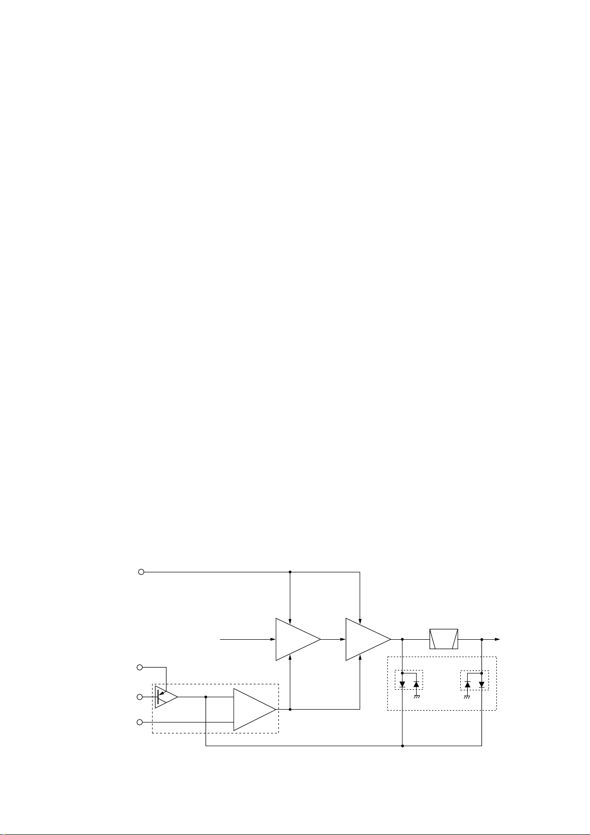
4-1-4 2ND IF AND DEMODULATOR CIRCUITS
The 2nd mixer circuit converts the 1st IF signal into a 2nd IF
signal. Adouble conversion superheterodyne system (which
converts receive signals twice) improves the image rejection
ratio and obtains stable receiver gain.
The 1st IF signal from the IF amplifier is applied to the 2nd
mixer section of the FM IF IC (IC2, pin 16), and is mixed with
the 2nd LO signal to be converted into a 450 kHz 2nd IF signal.
The FM IF IC contains the 2nd mixer, limiter amplifier, quadrature detector and active filter circuits. A 2nd LO signal
(45.9 MHz) is produced at the PLL circuit by tripling it’s reference frequency.
The 2nd IF signal from the 2nd mixer (IC2, pin 3) passes
through a ceramic filter (FI2) to remove unwanted heterodyned frequencies. It is then amplified at the limiter amplifier (IC2, pin 5) and applied to the quadrature detector (IC2,
pins 10, 11) to demodulate the 2nd IF signal into AF signals.
• 2ND IF AND DEMODULATOR CIRCUITS
Mixer
16
Limiter
amp.
2nd IF filter
450 kHz
PLL IC
IC1
X4
15.3 MHz
IC2 TA31136F
12
1st IF from the IF amplifier (Q14)
«SD» signal to the CPU pin 98
11109
87 5 3
AF signal «DET»
R5
X3
R86
C122
C121
R88R87
R83
«SQLIN» signal to the
D/A convertor (IC10, pin 23)
R82
C112 C113
C116
2
17 16
Active
filter
FI2
Noise
detector
FM
detector
13
«NOIS» signal to the CPU pin 19
RSSI
Noise
comp.
×3
R84
4 — 2
4-1-5 AF CIRCUIT
AF signals from the FM IF IC (IC2, pin 9) are applied to the
mute switch (IC4, pin 1) via the AF filter circuit (IC3b, pins 6,
7). The output signals from pin 11 are applied to the AF
power amplifier (IC5, pin 4) after being passed through the
[VOL] control (R143).
The applied AF signals are amplified at the AF power amplifier circuit (IC5, pin 4) to obtain the specified audio level. The
amplified AF signals, output from pin 10, are applied to the
internal speaker (SP1) as the “SP” signal via the [SP] jack
when no plug is connected to the jack.
4-1-6 SQUELCH CIRCUIT
Asquelch circuit cuts out AF signals when no RF signals are
received. By detecting noise components in the AF signals,
the squelch switches the AF mute switch.
Aportion of the AF signals from the FM IF IC (IC2, pin 9) are
applied to the active filter section (IC2, pin  where noise
components are amplified and detected with an internal
noise detector.
The active filter section amplifies noise components. The filtered signals are rectified at the noise detector section and
converted into “NOIS” (pulse type) signals at the noise comparator section. The “NOIS” signal is applied to the CPU
(IC8, pin 19).
The CPU detects the receiving signal strength from the
number of the pulses, and outputs an “RMUT” signal from
pin 49. This signal controls the mute switch (IC4, pin 13) to
cut the AF signal line.
4-2 TRANSMITTER CIRCUITS
4-2-1 MICROPHONE AMPLIFIER CIRCUIT
The microphone amplifier circuit amplifies audio signals with
+6 dB/octave pre-emphasis characteristics from the microphone to a level needed for the modulation circuit.
The AF signals from the microphone are applied to the
microphone amplifier circuit (IC3c, pin 10). The amplified AF
signals are passed through the low-pass filter circuit (IC3d,
pins 13, 14) via the mute switch (IC4, pins 4, 3). The filtered
AF signals are applied to the modulator circuit after being
passed through the mute switch (IC4, pins 9, 8).
4-2-2 MODULATION CIRCUIT
The modulation circuit modulates the VCO oscillating signal
(RF signal) using the microphone audio signal.
The audio signals change the reactance of a diode (D404)
to modulate an oscillated signal at the VCO circuit (Q7, Q8).
The oscillated signal is amplified at the buffer-amplifiers (Q4,
Q6), then applied to the T/R switching circuit (D3, D4).
4-2-3 DRIVE/POWER AMPLIFIER CIRCUITS
The signal from the VCO circuit passes through the T/R
switching circuit (D3) and is amplified at the buffer (Q403,
Q3), pre-drive (Q2) and power amplifier (Q1) to obtain 4 W
of RF power (at 7.2 V DC). The amplified signal passes
through the antenna switching circuit (D1), and low-pass filter and is then applied to the antenna connector.
The bias current of the pre-drive (Q2) and the power amplifier (Q1) is controlled by the APC circuit.
4-2-5 APC CIRCUIT
The APC circuit (IC3a, Q37) protects the drive and the
power amplifiers from excessive current drive, and selects
HIGH or LOW output power.
The signal output from the power detector circuit (D32, D33)
is applied to the differential amplifier (IC3a, pin 2), and the
“T4” signal from the expander (IC10, pin 11), controlled by
the CPU (IC8), is applied to the other input for reference.
• APC CIRCUIT
Q1
Power
amp.
Q2
Driver
amp.
IC3a
+
–
VCC
RF signal
from PLL
to antenna
T4
TXC
Q37
S5
APC control circuit
Power detector
circuit (D32, D33)
D33 D32
L4
LPF
4 — 3
When the driving current is increased, input voltage of the
differential amplifier (pin 2) will be increased. In such cases,
the differential amplifier output voltage (pin 1) is decreased
to reduce the driving current.
4-3 PLL CIRCUIT
A PLL circuit provides stable oscillation of the transmit frequency and receive 1st LO frequency. The PLL output compares the phase of the divided VCO frequency to the reference frequency. The PLL output frequency is controlled by
the divided ratio (N-data) of a programmable divider.
The PLL circuit contains the VCO circuit (Q7, Q8). The oscillated signal is amplified at the buffer-amplifiers (Q6, Q5) and
then applied to the PLL IC (IC1, pin 2).
The PLL IC contains a prescaler, programmable counter,
programmable divider and phase detector, etc. The entered
signal is divided at the prescaler and programmable counter
section by the N-data ratio from the CPU. The divided signal
is detected on phase at the phase detector using the reference frequency.
If the oscillated signal drifts, its phase changes from that of
the reference frequency, causing a lock voltage change to
compensate for the drift in the oscillated frequency.
A portion of the VCO signal is amplified at the buffer-amplifier (Q4), and is then applied to the receive 1st mixer (Q13)
or transmit buffer-amplifier circuit (Q403) via the T/R switching diode (D3, D4).
4-4 POWER SUPPLY CIRCUITS
VOLTAGE LINE
• PLL CIRCUIT
Shift register
3
Prescaler
Phase
detector
Loop
filter
Programmable
counter
Programmable
divider
X4
15.3 MHz
45.9 MHz signal
to the FM IF IC
«DEV» signal from the
D/A convertor (IC10, pin 22)
when transmitting
16
Q7, Q8
VCO circuit
Buffer
Q6
Buffer
Q4
Buffer
Q5
3
4
5
PLST
SCK
SO
to transmitter circuit
to 1st mixer circuit
D4
D3
17
8
2
LINE
HV
VCC
CPU5
T5
R5
S5
OPT
DESCRIPTION
The voltage from the attached battery pack.
The same voltage as the HV line (battery volt-
age) which is controlled by the power swtich
([VOL] control).
Common 5 V converted from the VCC line by the
reference regulator circuit (IC6). The output voltage is applied to the CPU (IC8), the 5 V regulator circuit (Q18, Q19), reset circuit (IC11) and
etc.
5 V for transmitter circuits regulated by the T5
regulator circuit (Q22).
5 V for receiver circuits regulated by the R5 regulator circuit (Q21).
Common 5 V converted from the VCC line by the
S5 regulator circuit (Q18, Q19).
The same voltage as the CPU5 line for the
optional HM-46L, HM-75A or HS-51 through a
resistor (R132).
4 — 4
4-5 PORT ALLOCATIONS
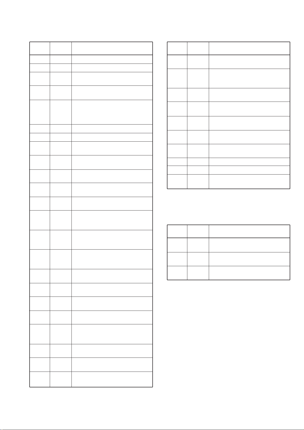
4-5-1 CPU (IC8)
Pin
number
1
9
11
12
15
16
17
18
19
21
36–38
44–47
49
50
51
52
53
54
55
56
57
58
59
Port
name
VIN
RESET
CSIFT
SCK
DAST
CLIN
CLOUT
PLST
NOIS
BUSY
OPV3–
OPV1
KR3–
KR0
RMUT
MMUT
DUSE
S5C
R5C
T5C
TXC
AFON
LIGT
ESCK
ESDA
Description
Input port for battely voltage detection.
Input port for RESET signal.
Outputs reference oscillator for the
CPU control signal.
Outputs clock signal to the PLL IC
(IC1), EEPROM (IC7), etc.
• Outputs strobe signals to the
expander IC (IC10, pin 6).
• Input port for the initial version signal.
Input port for the cloning signal.
Outputs the cloning signal.
Outputs strobe signals to the PLL IC
(IC1, pin 3).
Input port for noise signals (pulse
type).
Outputs BUSY detection.
Low: The channel is busy.
Input ports for the optional unit detection signal from J5.
Output ports for key matrix.
Low: When the key is pushed.
• Outputs RX mute control signal.
• Input port for the RX mute signal
from optional units.
• Output TX mute control signal.
• Input port for the TX mute signal
from optional units.
Outputs low-pass filter cut-off frequency control signal when DTCS is activated.
Outputs S5 regulator control signal.
Low: While power is ON.
Outputs R5 regulator control signal.
Low: While receiving.
Outputs T5 regulator control signal.
Low: While transmitting.
Outputs APC circuit control signal.
High: While transmitting.
Outputs control signal for the regulator
circuit of AF power amplifier.
High: When squelch is open, etc.
Outputs LCD backlight control signal.
High: Lights ON.
Outputs EEPROM (IC7, pin 6) clock
signal.
I/O port for data signals from/to EEPROM (IC7, pin 5)
Pin
number
63
90
91
94
95
96
97
98
99
100
Port
name
UNLK
MTONE
DTMF
CTCIN
PTT
BDET
REM0
SD
LVIN
TEMP
Description
Input port for unlock signal.
High:PLL is unlocked.
Output port for:
Beep audio while receiving.
2/5-tone signals while transmitting.
Outputs DTMF tone signal while transmitting.
CTCSS/DTCS signals input port for
decording.
Input port for the [PTT] switch.
High:While [PTT] switch is pushed.
Input port for the battery’s type detection.
Input port for the remote-control signal
from external MIC (HM-75).
Input port for the RSSI detection.
Input port for the PLL lock voltage.
Input port for the transceiver’s internal
temperature detection.
4-5-2 OUTPUT EXPANDER IC (IC10)
Pin
number
2, 3,
10, 11
6
7
Port
name
T1–T4
DAST
SCK
Description
Output tunable bandpass filter control
signals.
Input port for strobe signal from the
CPU (IC8, pin 15).
Input port for clock signal from the
CPU (IC8, pin 12).
CPU (IC8)–continued
Loading…
Document Download |
‹
›
Icom IC-F4GS Manual Online:
3.5,
729
votes
Icom IC-F4GS User Manual
Icom IC-F4GS User Guide
Icom IC-F4GS Online Manual
Text of Icom IC-F4GS User Guide:
More Instructions:
|
Icom IC-F4GS Instruction manual
|
DOWNLOAD | |
|
Icom IC-F4GS Instruction manual
|
DOWNLOAD | |
|
Icom IC-F4GS Servise manual
|
DOWNLOAD |
Related Products and Documents (Transceiver):
-
Icom IC-A210E Transceiver Instruction manual
IC-A210E
icom/ic-a210e.pdf, 40 -
Icom IC-91A Transceiver Instruction manual
IC-91A
icom/ic-91a.pdf, 131 -
Icom ID-1 Transceiver Instruction manual
ID-1
icom/id-1.pdf, 124 -
Icom IC-F3GS Transceiver Instruction manual
IC-F3GS
icom/ic-f3gs.pdf, 16 -
Icom IC-A3 Transceiver Instruction manual
IC-A3
icom/ic-a3.pdf, 47 -
Icom IC-F5020 Series Transceiver Instruction manual
IC-F5020 Series
icom/ic-f5020-series.pdf, 24 -
Icom iF5061D Transceiver Instruction manual
iF5061D
icom/if5061d.pdf, 32 -
Icom IC-E90 Transceiver Instruction manual
IC-E90
icom/ic-e90.pdf, 100
Comparable Devices:
| # | Manufacturer | Model | Document Type | File | Updated | Pages | Size |
|---|---|---|---|---|---|---|---|
| 1 | AL-KO | 426 036 | Manual | al-ko/426-036-681.pdf | 21 Oct 2024 | 25 | 3.38 Mb |
| 2 | green ecotherm | GP 45 IV | Manual | green-ecotherm/gp-45-iv-R85.pdf | 22 Sep 2023 | 53 | |
| 3 | Electro-Voice | QRx 212/75 | Specifications | electro-voice/qrx-212-75-8Q2.pdf | 17 Aug 2023 | 2 | 0.12 Mb |
| 4 | CYP | RAX-PSU-48V | Operation manuals | cyp/rax-psu-48v-SCD.pdf | 24 Jan 2024 | 20 | |
| 5 | JVC | KD-AV7010 — DVD Player With LCD Monitor | Installation & connection manual | jvc/kd-av7010-dvd-player-with-lcd-monitor-KVU.pdf | 19 Mar 2024 | 6 | |
| 6 | Sony | KDL-19M4000/B — Bravia M Series Lcd Television | Specification sheet | sony/kdl-19m4000-b-bravia-m-series-lcd-television-5M5.pdf | 22 Oct 2023 | 2 | 0.34 Mb |
Similar Resources:
Transceiver Instructions:
-
Farenheit Car Video System T-7020CMM
T-7020CMM (Car Video System ePDF User Guide, #I7ZI78)
T-7020CMM, 17
-
Intel Motherboard BLKDG45FC
Motherboard PDF Technical product specification
BLKDG45FC, 88
-
Electro-Voice Portable Speakers SH15-2
Electro-Voice Portable Speakers SH15-2 Specification sheet
SH15-2, 3
-
Philips Flat Panel TV 32PFL5203S/98
Philips Flat Panel TV Specifications (File: philips-32pfl5203s-98-operation-user-s-manual-3, Sunday 01-12-2024)
32PFL5203S/98, 3
-
Montigo Indoor Fireplace C34-BV
Manual: Montigo C34-BV (2L7CA6, Upd.Sun 10.2024)
C34-BV, 14
-
Clarion Keypad iClock 560
Keypad PDF Instructions manual
iClock 560, 28
-
Cisco IP Phone 7920 — Unified Wireless IP Phone VoIP
Cisco 7920 — Unified Wireless IP Phone VoIP User Manual (Configuring), @C7J44V
7920 — Unified Wireless IP Phone VoIP, 54
-
JVC Car Speakers CS-HX7158
JVC CS-HX7158 Guide (Doc Type: Car Speakers Instructions)
CS-HX7158, 2
-
Electrolux Other CYCLONE ULTRA
#TAJI9Z CYCLONE ULTRA: Electrolux Other Owner Documentation
CYCLONE ULTRA, 14
-
Goodman Furnace GRL SERIES
Goodman GRL SERIES Manual (Installation instructions manual), @9A1R92
GRL SERIES, 52
-
Jabra Headphone GN 4140
User Manual: Jabra GN 4140 (A9UKN8, Upd.Tue 10.2024)
GN 4140, 2
-
Suzuki Outboard Motor GF60A
GF60A Service manual — C3NI11
GF60A, 336
Comments, Questions and Opinions:
Icom IC-F4GS Transceiver PDF User Guides and Manuals for Free Download: Found (4) Manuals for Icom IC-F4GS Device Model (Servise Manual, Instruction Manual)
The Icom IC-F4GS is a robust handheld radio that has garnered a solid reputation among communication enthusiasts and professionals alike. It is primarily recognized for its durability, ease of use, and a range of features that cater to various communication needs. In this review, we’ll delve into the key aspects of the IC-F4GS, examining its build quality, performance, usability, and the value it provides for its price point.
One of the standout features of the Icom IC-F4GS is its rugged construction. Designed to withstand harsh conditions, this radio is compliant with IP54 and MIL-STD-810 standards. Whether you’re in a challenging work environment or an outdoor adventure, the IC-F4GS can endure water splashes and dust, ensuring reliable performance when it matters most.
Performance-wise, the IC-F4GS is impressive. With a frequency range of 136 to 174 MHz, it offers VHF coverage that is ideal for various communication applications, from industrial usage to recreational activities. The radio supports both analog and digital modes, allowing flexibility depending on user needs.
Battery life is another crucial aspect where the Icom IC-F4GS excels. It comes with a high-capacity battery that provides extended operational time, minimizing interruptions during use. Users can rely on the IC-F4GS for long shifts or extended outdoor activities without frequently worrying about recharging.
Usability is another area where this radio shines. The Icom IC-F4GS features a straightforward interface coupled with intuitive buttons, making it easy for both novices and experienced users to navigate. The LCD display is clear, ensuring that information is easily readable even in bright sunlight or low-light conditions. The menu settings are user-friendly, allowing for quick adjustments without extensive manual referencing.
Key Features of the Icom IC-F4GS:
- Durable Design: IP54 and MIL-STD-810 compliant.
- Wide Frequency Range: 136 to 174 MHz VHF.
- Long Battery Life: High-capacity battery for extended usage.
- Versatile Modes: Supports both analog and digital communication.
- Easy to Use: User-friendly interface and clear LCD display.
Moreover, the IC-F4GS comes equipped with powerful audio capabilities, allowing for loud and clear communication even in noisy environments. This is particularly beneficial for individuals working in construction, security, or outdoor event management where clear communication is crucial to maintaining efficiency and safety.
However, it is essential to consider a few minor drawbacks. Some users have noted that the size and weight of the IC-F4GS might not be the most pocket-friendly option for extended carrying. Additionally, while the radio supports various frequencies and modes, beginners may initially find some of the advanced features overwhelming without proper training.
In conclusion, the Icom IC-F4GS is an excellent choice for anyone seeking a reliable and robust handheld radio. With its combination of durability, excellent performance, and user-friendly design, it stands out in a competitive market. Whether for professional work or personal use, the IC-F4GS ensures that communication remains uninterrupted, secure, and effective. Overall, it represents a solid investment for anyone requiring a dependable communication tool.
FAQ: Types of Manuals and Their Contents
Icom IC-F4GS Manuals come in various types, each serving a specific purpose to help users effectively operate and maintain their devices. Here are the common types of Icom IC-F4GS User Guides and the information they typically include:
- User Manuals: Provide comprehensive instructions on how to use the device, including setup, features, and operation. They often include troubleshooting tips, safety information, and maintenance guidelines.
- Service Instructions: Designed for technicians and repair professionals, these manuals offer detailed information on diagnosing and repairing issues with the device. They include schematics, parts lists, and step-by-step repair procedures.
- Installation Guides: Focus on the installation process of the device, providing detailed instructions and diagrams for proper setup. They are essential for ensuring the device is installed correctly and safely.
- Maintenance Manuals: Provide guidance on routine maintenance tasks to keep the device in optimal condition. They cover cleaning procedures, part replacements, and regular servicing tips.
- Quick Start Guides: Offer a concise overview of the essential steps needed to get the device up and running quickly. They are ideal for users who need immediate assistance with basic setup and operation.
Each type of Icom IC-F4GS instruction is designed to address specific needs, ensuring users have the necessary information to use, maintain, and repair their devices effectively.
Related Instructions for Icom IC-F4GS:
5
IC-V210T
Instruction manual Icom Transceiver Instruction manual (File: icom-ic-v210t-instruction-manual-16, 17/11/2024)
16
763
191
7
IC-207H
Instruction manual Icom Transceiver Instruction manual (File: icom-ic-207h-instruction-manual-13, 12th Mar 2025)
13
201
41
Transceiver Devices by Other Brands:
|
AUREL XTR-8LR-USB Operation & User’s Manual PDF User Guide (@81S4TP), AUREL XTR-8LR-USB Transceiver (Monday 10-03-2025) XTR-8LR-USB 10 Mar 2025 | 17 |
|
|
IMC Networks Copper SFPs Features And Benefits IMC Networks Transceiver Features and benefits (File: imc-networks-copper-sfps-features-and-benefits-2, Monday 14-04-2025) 800-624-1070 14 Apr 2025 | 2 |
|
|
Kenwood TK-3312 Service Manual Kenwood TK-3312 Guide (Service manual), @3E3XO9 SERVICE MANUAL 19 Nov 2024 | 52 |
|
|
Yaesu FT-1802M Specifications Transceiver #3Q99B2 FT-1802M/E 04 Nov 2024 | 2 |
Categories:
Network Card
Tuner
Vhf transceiver
Sander
Amplifier
TV Receiver
The Icom IC-F4GS is a top-tier handheld transceiver designed for professional use in demanding environments. This device is built for durability, featuring a rugged construction that meets military specifications for water and dust resistance. Users can trust the IC-F4GS to perform in challenging conditions, whether it be during outdoor adventures or in industrial settings. Here, we will explore the specifications, features, and overall performance of the Icom IC-F4GS.
Specifications:
- Frequency Range: VHF 136-174 MHz, UHF 400-470 MHz
- Power Output: 5W (high), 1W (low)
- Battery Life: Up to 18 hours with a 2000mAh battery
- Weight: Approximately 330 grams (with battery)
- Dimensions: 120mm x 56mm x 36mm
- Waterproof Rating: IP54/55
- Operating Temperature: -20 to +60 degrees Celsius
The Icom IC-F4GS stands out with its impressive power output capabilities. With a maximum power of 5 watts in high mode and the option to switch to 1 watt for more conservative use, this device offers versatility for various communication needs. This is particularly beneficial for users who require reliable communication over short distances without the need for high power. The extended battery life allows users to stay connected for extended periods, which is ideal for long shifts or outdoor activities.
Key Features:
- Diverse Communication Modes: The device supports both analog and digital modes, allowing for seamless communication across different platforms.
- User-Friendly Interface: The backlit LCD display is large and clear, making it easy to navigate menus and settings even in low-light conditions.
- Built-in VOX Functionality: This feature enables hands-free operation, making it particularly useful for users engaging in activities that require multitasking.
- Channel Memory: The IC-F4GS offers 128 memory channels, which can be programmed for quick access to frequently used frequencies.
- Busier Environments: Equipped with an automatic noise limiter and various filtering options, the IC-F4GS enhances audio clarity in noisy environments, ensuring that users can communicate effectively.
Overall, the Icom IC-F4GS is a robust choice for professionals who demand quality performance in a handheld transceiver. Its combination of advanced features, durable design, and user-friendly interface makes it suitable for a variety of applications, including public safety, construction, and outdoor adventures. Moreover, Icom has established a strong reputation in the communication device market, and the IC-F4GS upholds this standard of excellence.
In conclusion, for anyone looking for a reliable and feature-rich handheld radio, the Icom IC-F4GS is certainly worth considering. Its impressive specifications, along with its versatility and durability, make it a leading option for users needing dependable communication tools in any setting.
Related IC-F4GS Manuals and Guides
Type: Sales handbook
Brand: Icom
Category: Transceiver
Pages: 39
Type: Operating manual
Brand: Icom
Category: Transceiver
Pages: 46
Type: Service manual
Brand: Icom
Category: Transceiver
Pages: 59
Type: Firmware update
Brand: Icom
Category: Transceiver
Pages: 28
Type: Instruction manual
Brand: Icom
Category: Transceiver
Pages: 52
Type: Instruction manual
Brand: Icom
Category: Transceiver
Pages: 51
Type: Operating manual
Brand: Icom
Category: Transceiver
Pages: 26
Type: Instruction manual
Brand: Icom
Category: Transceiver
Pages: 40
Type: Instruction manual
Brand: Icom
Category: Transceiver
Pages: 132
Type: Instructions
Brand: Icom
Category: Transceiver
Pages: 2
Type: Service manual
Brand: Kenwood
Category: Transceiver
Pages: 33
Type: Instruction manual
Brand: Midland
Category: Transceiver
Pages: 30